-
U heeft nog geen producten in uw winkelwagen.
U heeft nog geen producten in uw winkelwagen.
Wide bandgap semiconductors like silicon carbide (SiC) and gallium nitride (GaN) not only excel at high-temperature and high-voltage endurance, but also offer low losses and very high switching frequencies. However, to truly harness the advantages of these advanced materials, extremely precise testing and measurement techniques are essential. In particular, in Double Pulse Test (DPT), optically isolated probes not only ensure the safety of the measurement process, but also enhance accuracy and reliability. In this article, we explain why the optical isolation probe is truly indispensable in double pulse testing.
Double Pulse Test (DPT) is an experimental method used to evaluate the switching performance of power electronic devices, such as Insulated Gate Bipolar Transistors (IGBTs) or MOSFETs (Metal-Oxide-Semiconductor Field-Effect Transistors). The test applies two short voltage pulses to the device, simulating its real switching behavior in circuit operation. It is used to measure and analyze the device’s switching characteristics, optimize gate driver and application design, and for fault diagnosis or simulation model validation.
Taking the half-bridge gate driver for MOSFETs as an example, you need to measure the lower MOSFET’s Vds, Id, and Vgs, as well as observe the Vgs of the upper MOSFET. The Micsig MHO high-resolution oscilloscope series (up to 500MHz bandwidth, 3GSa/s sampling, ≤1% accuracy, 4-channel simultaneous observation) perfectly meets the requirements for Double Pulse Testing.

For accurate Id waveform measurement, it is crucial that the current probe offers sufficient bandwidth. The Micsig CP series of AC/DC current probes provide up to 100MHz bandwidth, accuracy within 1%, resolution up to 1mA, and can measure up to 30A. For even higher currents, the Rogowski RCP current probes can be used.
However, many users ask: “We have Micsig DP differential probes, which work well for silicon devices up to 7000V and 500MHz. Now that we’re using GaN and SiC, these should theoretically suffice. Indeed, they work for the lower MOSFET. But why do we always run into issues measuring the voltage on the upper MOSFET?”
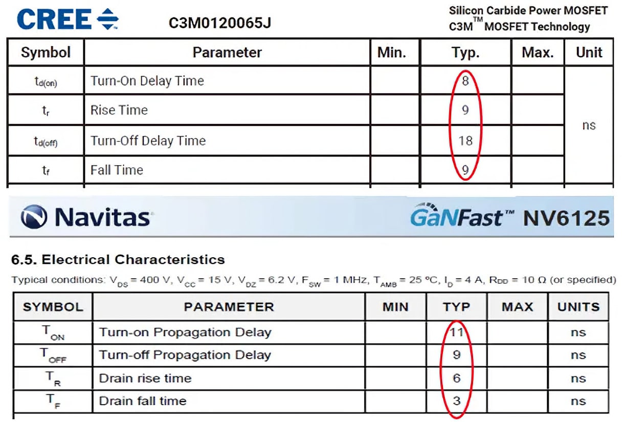
As shown in the data, SiC and GaN switches reach nanosecond-level switching speeds. This reduces switching losses in converters, but makes measurement extremely challenging: in the half-bridge, the high-side MOSFET’s Vgs “floats” during Vds transitions, which can swing from zero to thousands of volts in just a few nanoseconds. The combination of high voltage and frequency generates significant high-order harmonics. The actual Vgs differential signal is often just tens of volts, but suffers heavy common-mode interference from Vds harmonics. You need to suppress this as much as possible, and only instruments with high CMRR even at high frequency can succeed.
For reference, the DP series: at 100kHz, CMRR is > -70dB; at 20MHz > -40dB; at 120MHz > -26dB. These are excellent differential probe values, but still not enough for high-frequency measurement of the upper MOSFET Vgs: you need a probe that maintains extremely high CMRR even at those frequencies.
To see the effect of CMRR on measurement, let’s compare high-voltage differential probes and optically isolated probes, highlighting problems that arise in measurement.
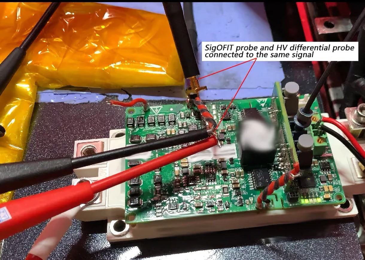
Method: A SiC switch at about 500V Vce is tested with both a high-voltage differential probe (Micsig DP) and optically isolated probe (Micsig SigOFIT) connected in parallel to the upper gate Vge.
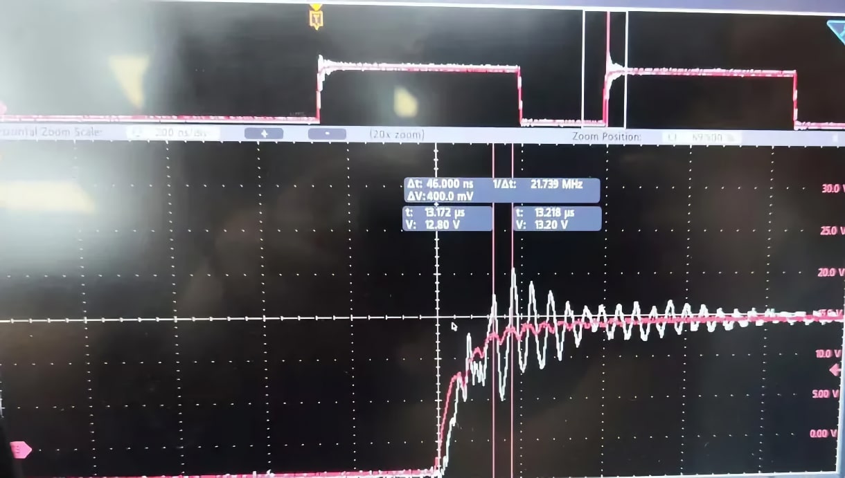
The white signal (differential probe) shows heavy oscillations on the Vge rising edge, making it impossible to distinguish the true waveform. Previously, measuring upper gate Vge with a differential probe on 800V Vce devices, the oscillation would exceed the device’s turn-off voltage, undermining engineer evaluation.
The red signal (optical probe) shows almost no interference. If used alone, the optical probe’s noise is virtually eliminated. Any residual interference in the figure is due to coupling from the differential probe. Optical probes provide lower baseline noise, higher accuracy, and can withstand higher common-mode voltages. How is this achieved?
Micsig’s exclusive SigOFIT™ technology allows you to select the optimal attenuator for the signal, covering ±0.01V up to ±6250V at full scale. This adaptation increases test accuracy (up to 1%), lowers the noise floor, and improves signal-to-noise ratio.
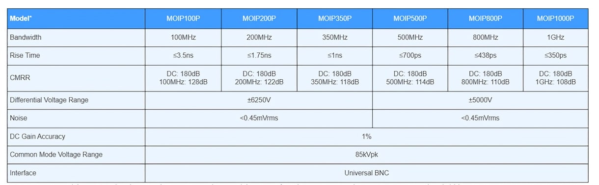
With bandwidth up to 1GHz, SigOFIT probe noise stays below 0.45mVrms. Even at 1GHz, CMRR remains above 100dB. Measuring high-side Vgs with the optical probe, you can virtually ignore common-mode interference and overcome the limitations of high-voltage differential probes.

Also, the lead length of differential probes (~20cm) acts as an antenna, sensitive to magnetic interference. Fast GaN devices can induce oscillations through the differential probe’s input, sometimes exceeding limits and causing device failure. SigOFIT optical probes use ultra-short MCX/MMCX leads, minimizing any antenna effect. Parasitic capacitance remains below a few pF, eliminating safety risks due to parasitic effects.
In summary, optically isolated probes surpass differential probes in every performance aspect. For users doing double pulse testing, the Micsig optical isolation probe is the best choice.


Leave a Comment